There are two types of TP processes, one is resistive screen and the other is capacitive screen. This article focuses on capacitive screen.
Professional Name Explanation:
LCM: Liquid Crystal Display
(TP): Capacitive Touch Screen.
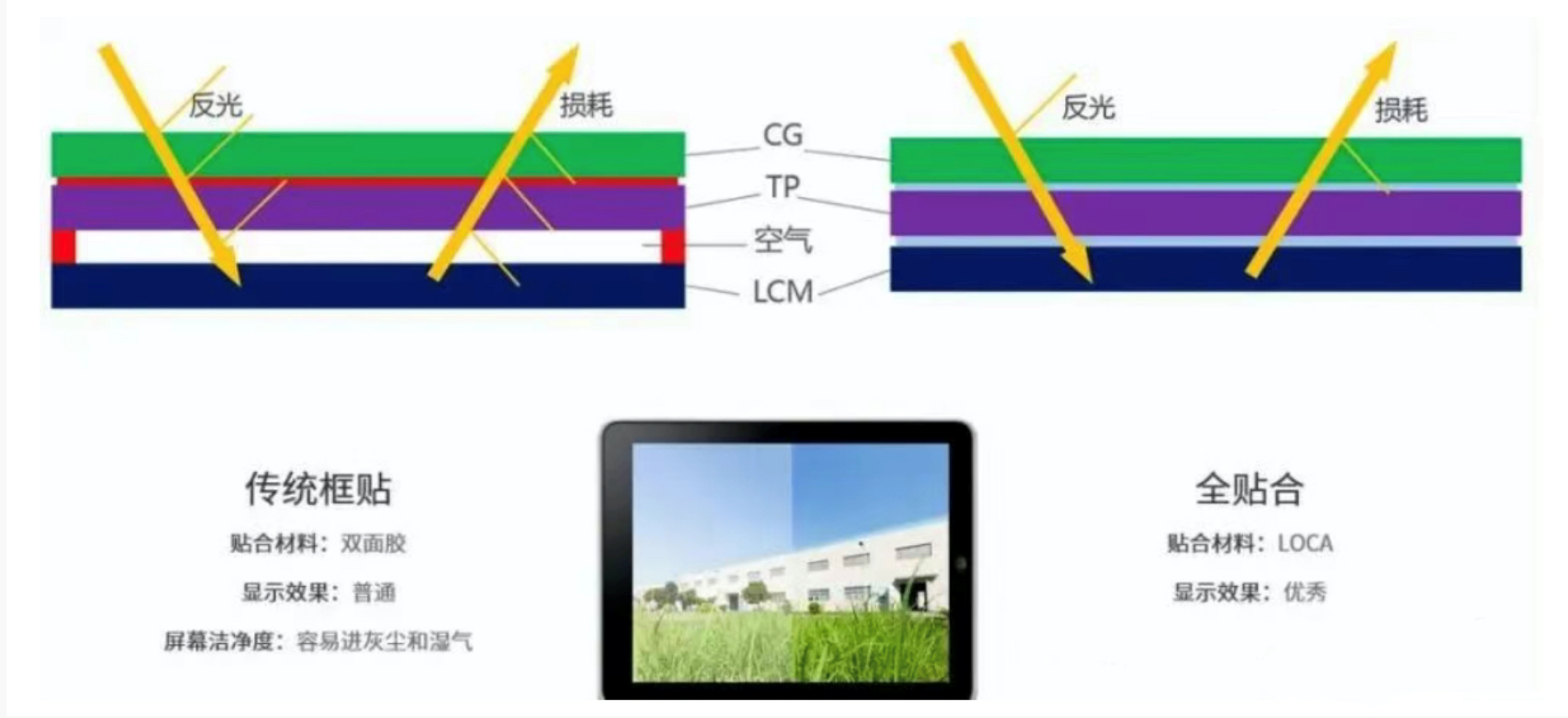
Air bonding: Double-sided tape applied to the TFT-LCD panel.
Optical bonding: OCA glue integrates the TP and LCM.
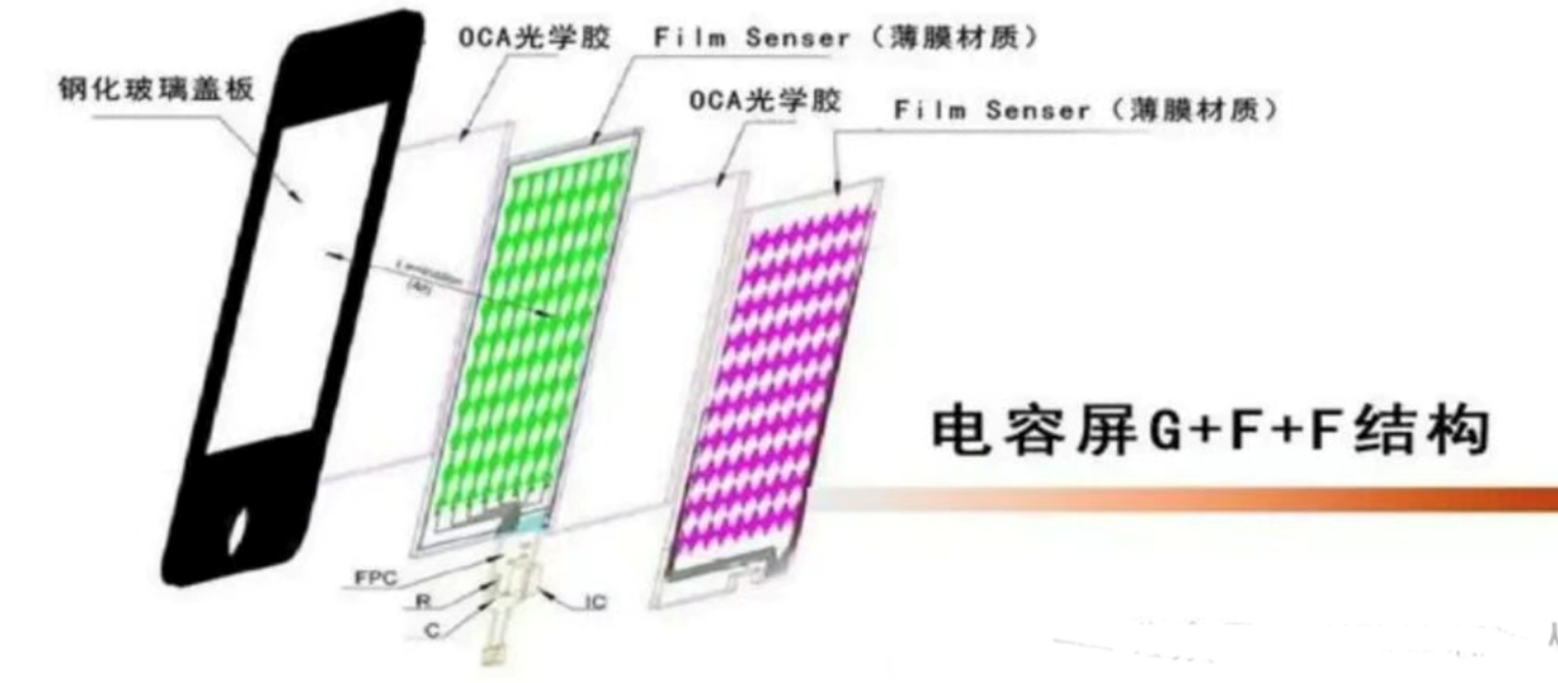
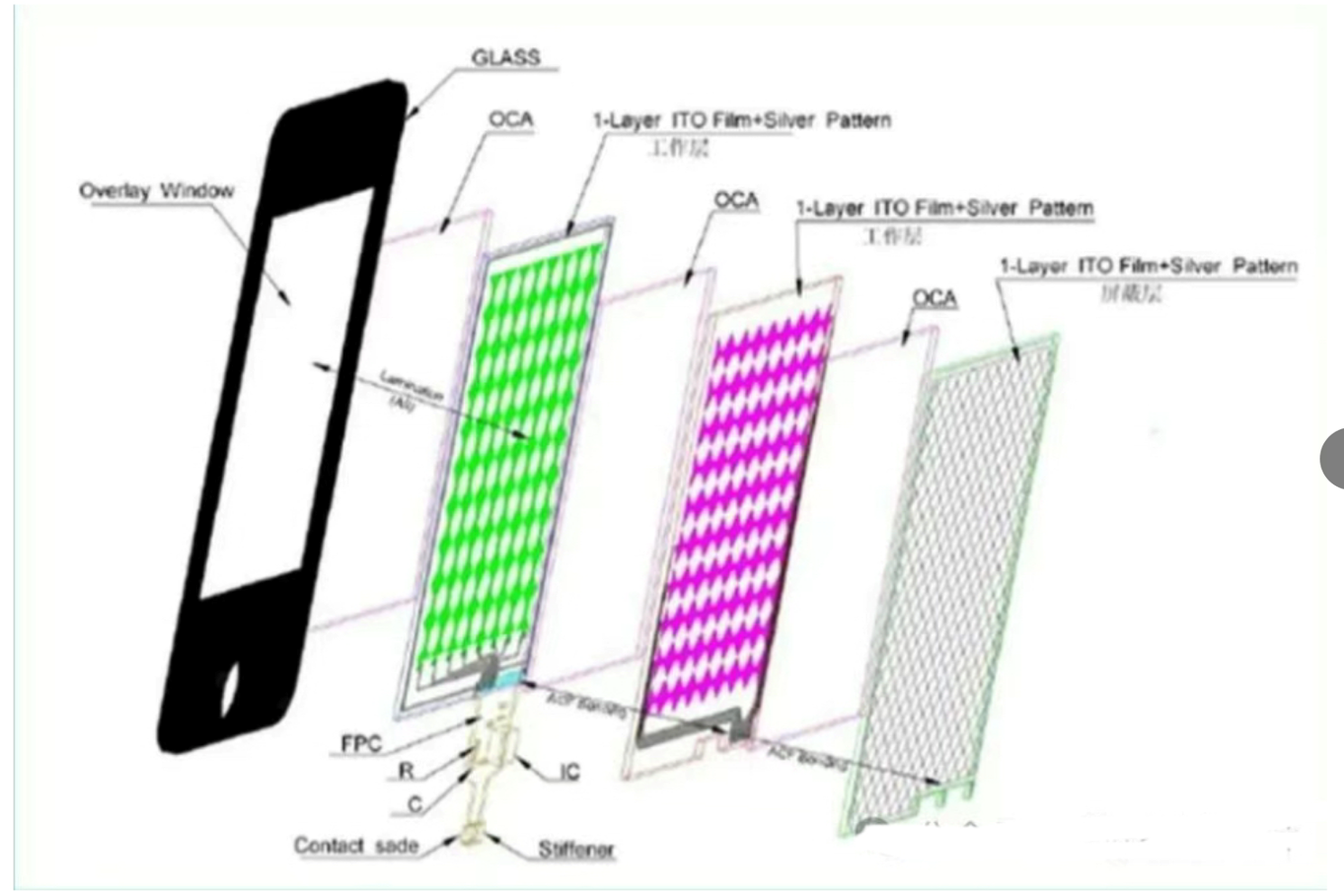
This is the structural classification of TP. The first letter represents the surface material (also known as the upper layer), and the second letter represents the touchscreen material (also known as the lower layer). The two are bonded together. G+G:
Surface tempered glass + touchscreen made of glass. G+P:
Surface tempered glass + touchscreen made of PC. G+F:
Surface tempered glass + touchscreen made of film.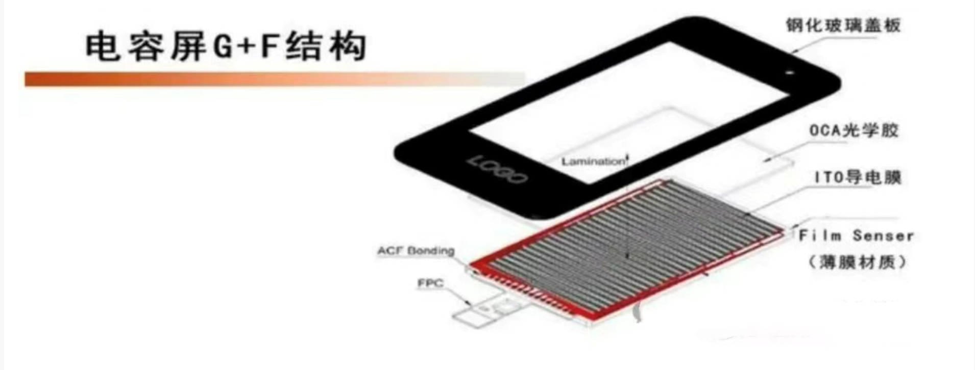

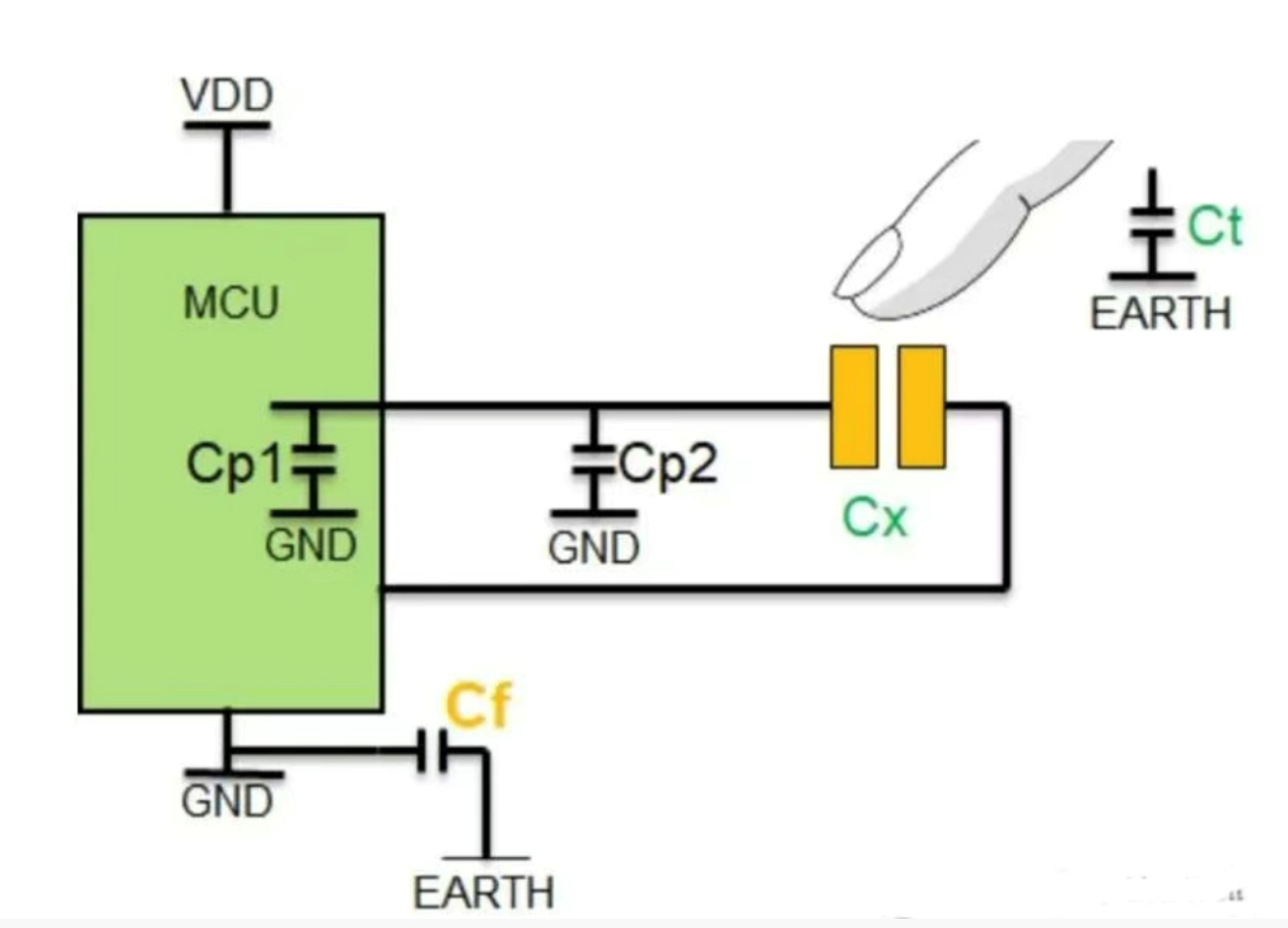
When a user touches the screen, the human body's electric field creates a coupling capacitor between the finger and the conductive layer. Current flows through the four electrodes, and the current strength is proportional to the distance between the finger and the electrodes. A significant problem with this principle is significant drift; even the slightest external interference can cause the touch screen to malfunction. I haven't seen this principle applied in any specific field yet.How Projected Capacitive Touchscreens Work
Basic Principle:
The touch screen utilizes multiple layers of ITO, arranged in a matrix. The X- and Y-axis cross-distribution serves as the capacitance matrix. When a finger touches the screen, the X- and Y-axis scans detect the change in capacitance at the touch location, allowing the finger's location to be determined. Based on this architecture, projected capacitive touchscreens enable multi-touch operation.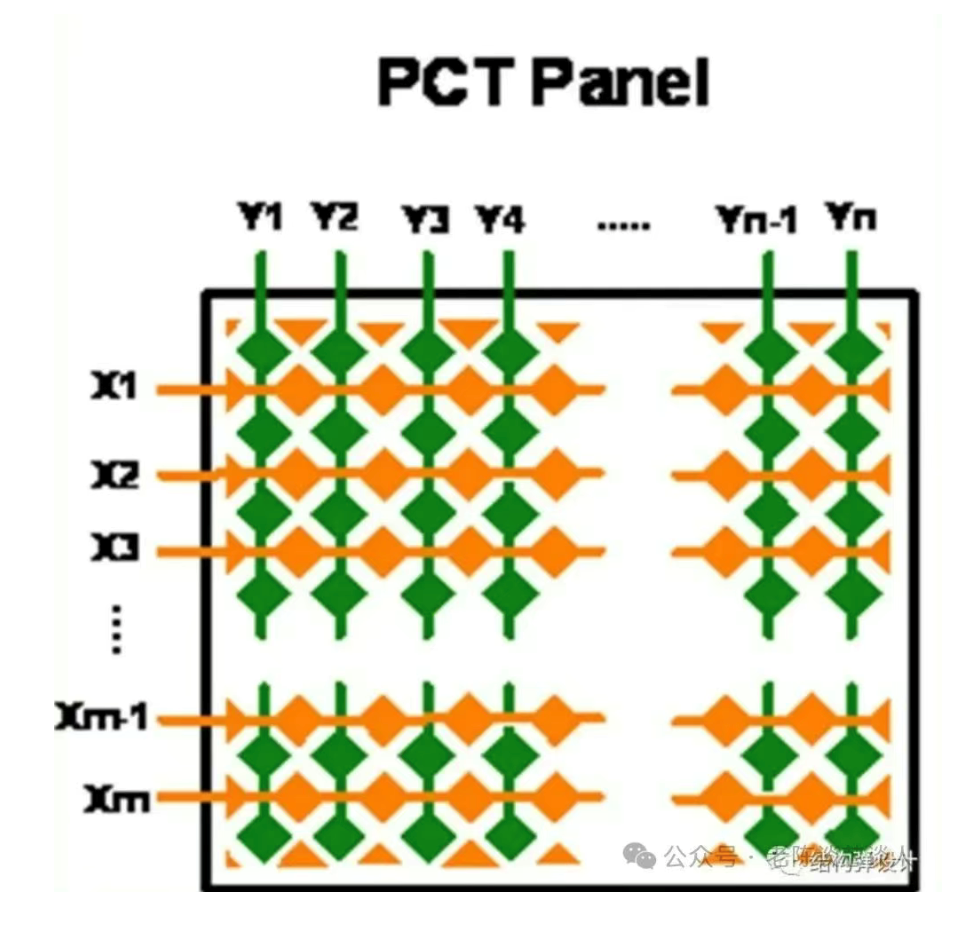
There are two types of projected capacitive sensors: self-capacitance and mutual capacitance. These two principles have been used in large quantities in consumer, industrial, automotive and other fields.Self-capacitance principle
Measure the change in capacitance between a single electrode and ground. Capacitance is scanned line by line, with all channels acting as both sensing and driving signal channels. By comparing the capacitance change before and after a touch, the X/Y coordinates are determined and then combined to form the coordinates of the touch poin
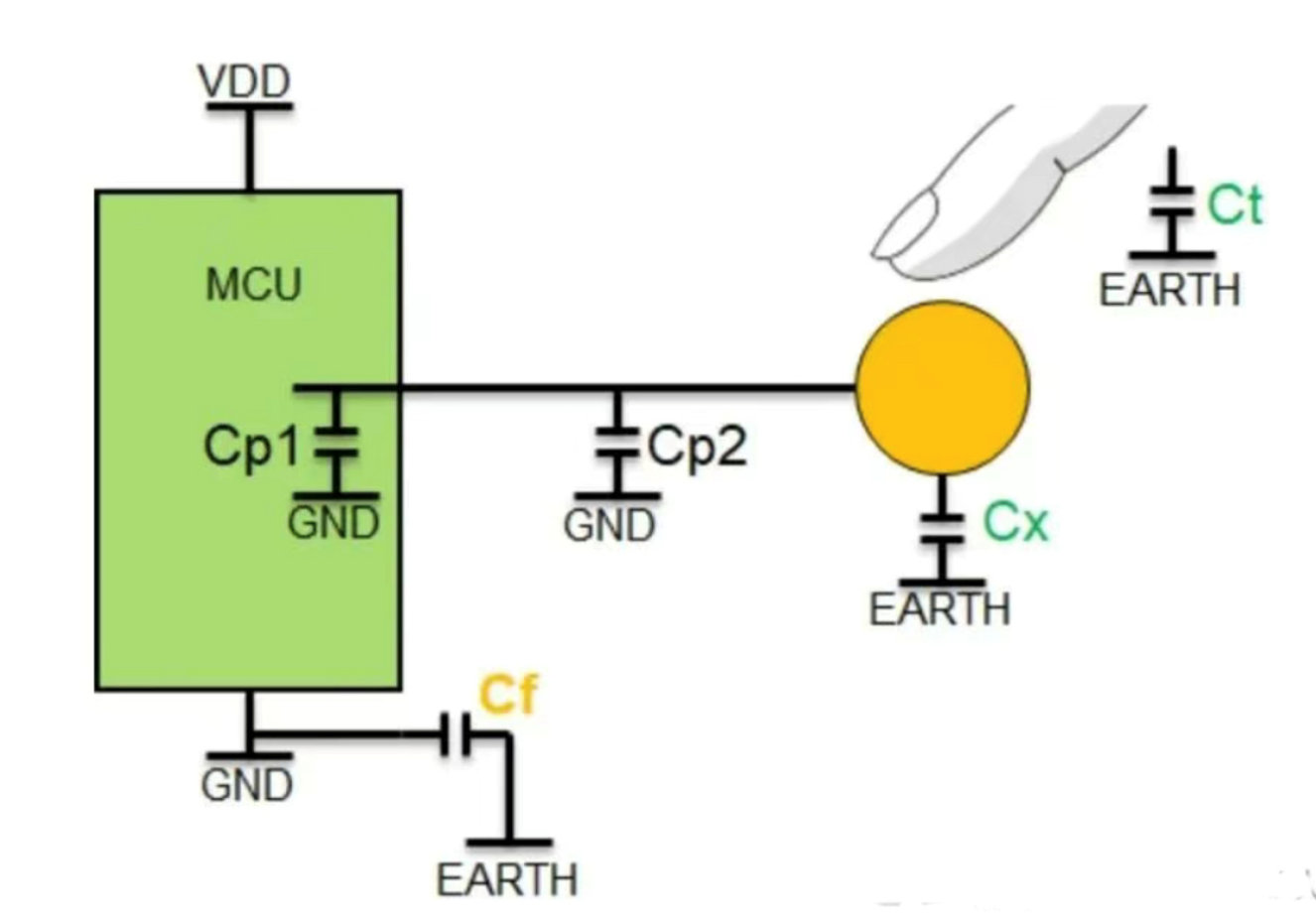
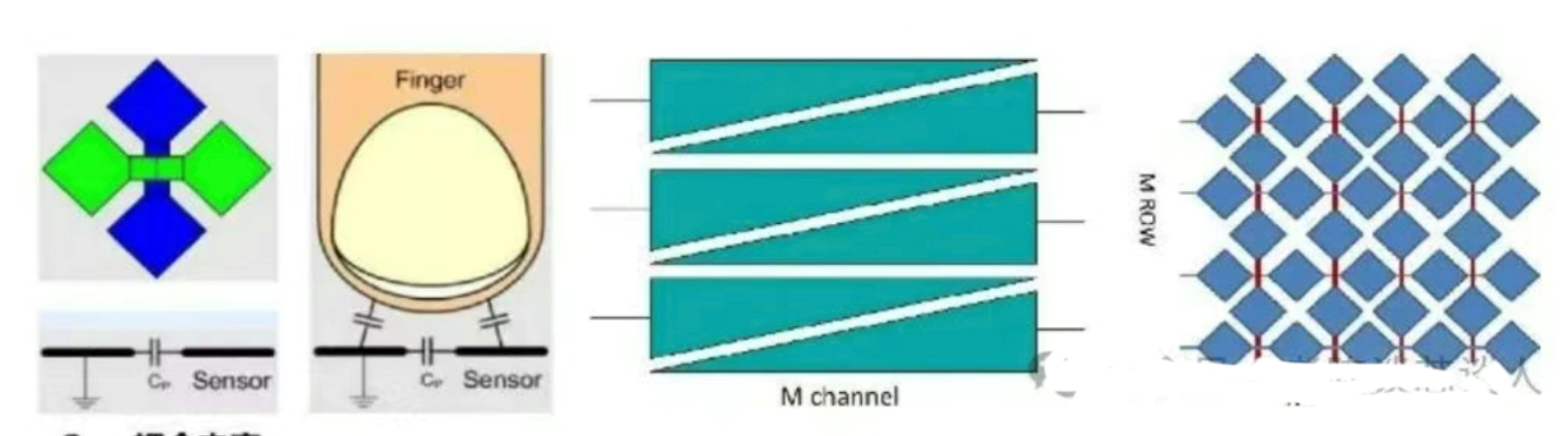
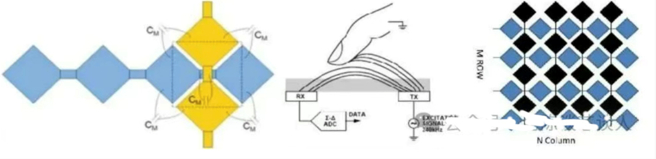
Measuring changes in the coupling capacitance between row and column electrodes. Mutual capacitance divides the X and Y channels into drive signal channels and sensing signal channels. The drive signal is sent row by row. After the first row drive signal is sent, the sensing signal channel scans row by row to determine whether there is a change in capacitance. When a touch is applied, it is like connecting a capacitor in series, so the capacitance decreases.
In-cell TP
Currently, screen manufacturers are promoting in-cell TP, which mainly includes the in-cell and once-cell processes. The main difference between in-cell/on-cell and external TP is that the TX/RX circuits are located inside the polarizer, meaning that the TP circuits are fabricated at different locations within the LCM.
In-cell: Touch circuits are fabricated directly between the front and back conductive glass of the panel (cell) (that is, inside the cell). This is called in-cell. Currently, the main technical structures are as follows:
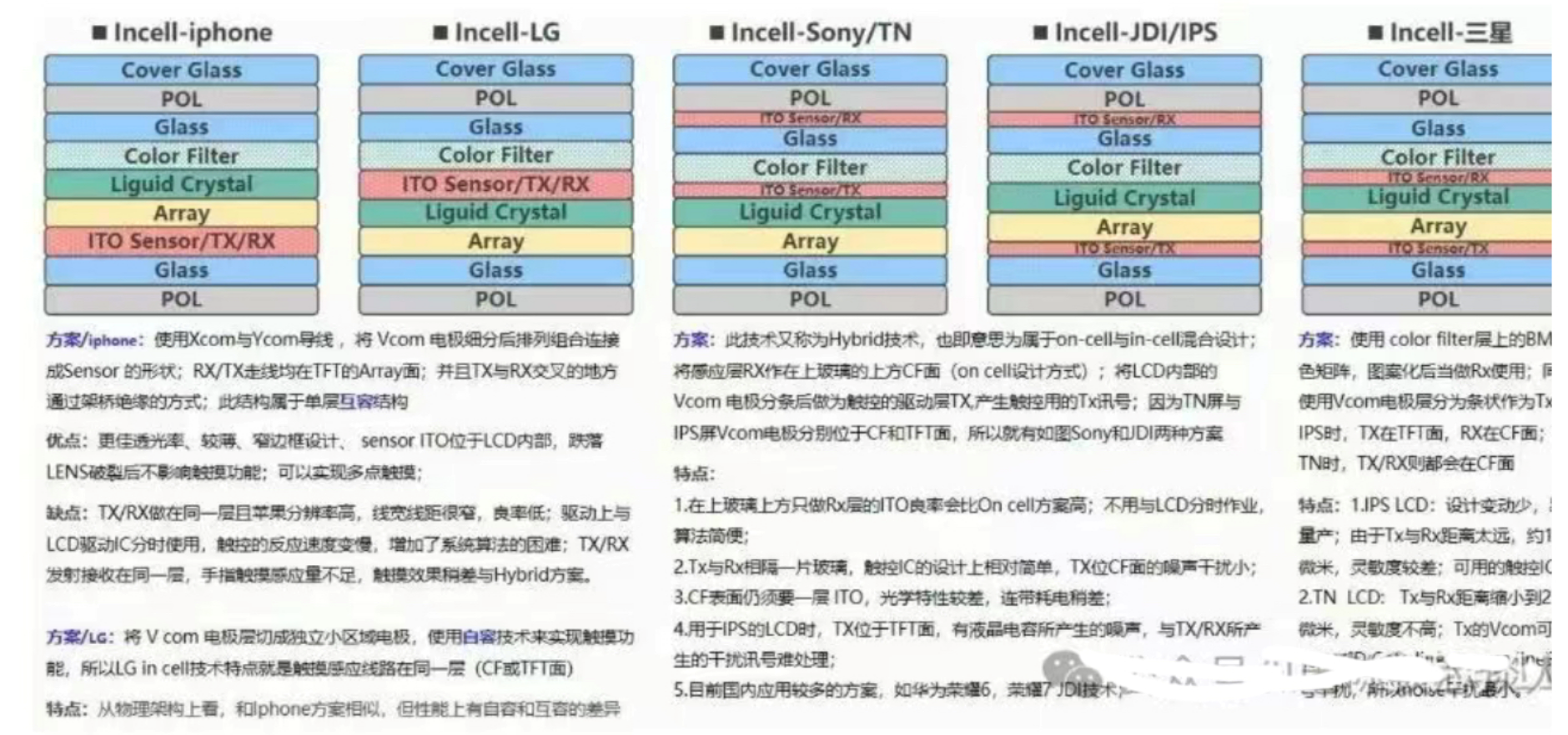
On-cell: The sensor circuit coating is made on the front conductive glass (CF) surface of the LCD, which is called On-cell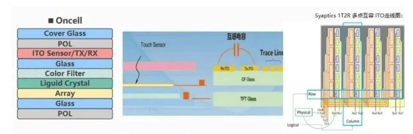 Touch performance
Touch performance GFF > Incell > GFM > ONCELL > GF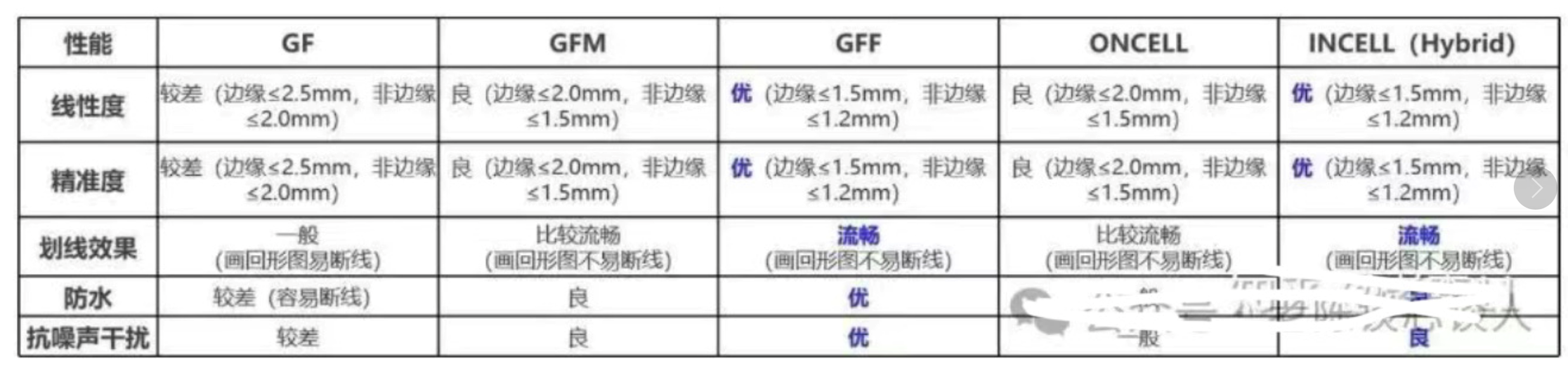 if you will have any tech. of LCD with PCAP issue, pls. kindly contact us